Dual-chip (spanned) BIOS - UEFI Crash Course Part 3
Chapters12
The creator admits miscounting the SPI header pins, correcting the method for reading headers and stressing correct pin orientation.
Adamant IT walks through a hands-on dual-chip BIOS schema, showing how to read, combine, and flash split BIOS images using pogo pins, UEFI Tool, and a capsule from Lenovo as a real-world test.
Summary
Adamant IT’s latest session dives into a practical dual-chip BIOS scenario, differentiating it from a true dual-BIOS setup. The host explains how two differently sized SPI flash chips can store a single BIOS image, with the main BIOS on the larger chip and auxiliary regions on the smaller one. He demonstrates hands-on techniques to identify which chip contains which data, reads both chips with pogo pins, and then combines their contents into a single 24 MB image. The video walks through extracting a Lenovo BIOS capsule, parsing the capsule with UEFI Tool, and separating the image into WindBond and QMC components. Throughout, Adamant IT emphasizes why older boards used dual chips (cost vs capacity) and why flashing may not immediately fix a laptop due to non-BIOS data like serial numbers. The practical workflow includes dumping chips, verifying regions, and preparing separate BIN files for each chip before flashing. He ends with reflections on why sometimes a clean ME region isn’t enough and teases the next video’s deeper dive into BIOS regions. The tone is instructional and grounded in a real-world repair scenario, with attention to pin counting, chip identification, and methodical data assembly rather than theoretical perfection.
Key Takeaways
- Dual-chip BIOS uses two SPI ROMs (e.g., 16 MB + 8 MB) to hold a single BIOS image, with main regions on the larger chip and descriptors/ME on the smaller one.
- Pogo-pin readers can effectively dump SPI ROMs in tight board layouts, provided you disable pin detect and correctly identify chip voltage (e.g., 3V for WindBond 25R64 JV).
- Combining two chips’ images into a single binary (e.g., 16 MB + 8 MB = 24 MB) enables analysis in UEFI Tool, revealing an Intel image with ME and descriptor regions.
- Lenovo/other OEM capsules can contain the full BIOS payload; extracting and isolating the Intel image from a capsule lets you get a clean flash file that matches the dual-chip layout.
- Flashing the ME-containing smaller chip first can sometimes stabilize power-on behavior enough to post, even if serial data remains to be re-provisioned later.
- Understanding why dual-chip BIOS exists includes cost-to-capacity considerations; a larger single chip may be pricier than pairing two smaller chips.
- The process often requires iterative validation: dump chips, open in UEFI Tool, attempt to reassemble, then reflash and reassess the laptop’s behavior.
Who Is This For?
Essential viewing for hardware enthusiasts, firmware engineers, and repair techs who want a concrete, hands-on guide to diagnosing, assembling, and flashing dual-chip BIOS images on laptops using SPI flash, pogo pins, and UEFI tools.
Notable Quotes
"This is a crash course, not a master class."
—Sets the tone for the troubleshooting-focused video and acknowledges the learning curve.
"I counted the pins completely wrong. I counted from left to right on both rows, which is just wrong on any kind of chip."
—Highlights a common hardware debugging error and emphasizes careful pin counting.
"Let's dump the contents of these two chips and see what we find on them."
—Demonstrates the core data-gathering step of dumping both SPI chips to analyze the BIOS split.
"We have a dual chip BIOS here. And we've just dumped both chips and then combined the contents into a single file."
—Confirms the core discovery and the practical action of merging two ROM dumps into one image.
"If you've got a high-speed programmer like an XG Pro, yeah, this is pretty decent."
—Offers a realistic appraisal of hardware tools used for flashing and validates the chosen approach.
Questions This Video Answers
- How do you identify which SPI chip in a laptop holds the main BIOS versus ME/descriptor regions?
- What is a capsule file in BIOS updates and how do you extract the payload for a dual-chip BIOS?
- Why would a motherboard use two SPI chips for BIOS firmware instead of one large chip?
- How do you safely flash only the ME region chip first when repairing BIOS on a laptop?
- What tools are needed to read and reconstruct dual-chip BIOS images from separated ROMs?
Dual-chip BIOSSPI flashPogo pinsBIOS capsuleUEFI ToolWindBondQMCIntel ME regionME firmwareLenovo BIOS update extraction
Full Transcript
On the previous video in this series, I showed you guys how to make a custom SPI header cable for flashing modern ATX motherboards. But for some reason or other, in the previous video, my one didn't work. Now, at the time, I put this down to the actual method being a little bit jank. These SPI headers aren't really standardized and are more of a sort of engineers debug port. Um, it's not intended to be used by the end user for BIOS flashing. So, I just assumed that there was some kind of oddity on this particular motherboard to do with pull-up resistors or something like that interfering with what I was trying to do.
Um, however, the comments section was very quick to spot my mistake. Despite me saying very explicitly in the video to be careful about how you count the pins on the chips, if you make up a pin header and it's not working, doublech check that you are counting pins in the correct direction for each header you're working with because they're all different. I counted the pins completely wrong. I counted from left to right on both rows, which is just wrong on any kind of chip. You either c you either move in columns or you move counterclockwise.
Now, I'd love to pretend that this was deliberate and I was just testing you all to make sure you were all paying attention and I'm very proud of you all for pointing out my error, but no, I just had a complete lapse of concentration and got it completely wrong in the demonstration. This is a crash course, not a master class. So, thank you for everyone else for spotting where I went wrong. I did pin the comment reasonably quickly, but I then spent the next two weeks dying of cringe. Moving on from that, we then had a quick look at an ASUS capsule file, which introduced us to UEFI tool and how we can look inside BIOS files as a package of regions and segments that we can edit and manipulate.
I want to expand on that a little bit further today by showing you a dual chip BIOS setup. Now, this isn't the same as a dual BIOS setup. Dual BIOS involves having two identical BIOS chips that function as either a main and a backup or two alternate BIOS profiles. High-end ATX motherboards often have a backup BIOS chip that it will auto select in the event of a boot failure, or it can sometimes be selected with a physical switch on the motherboard as well. Graphics cards will often have a second BIOS chip that stores a different overclocking profile, which again usually has a selector switch somewhere on the card.
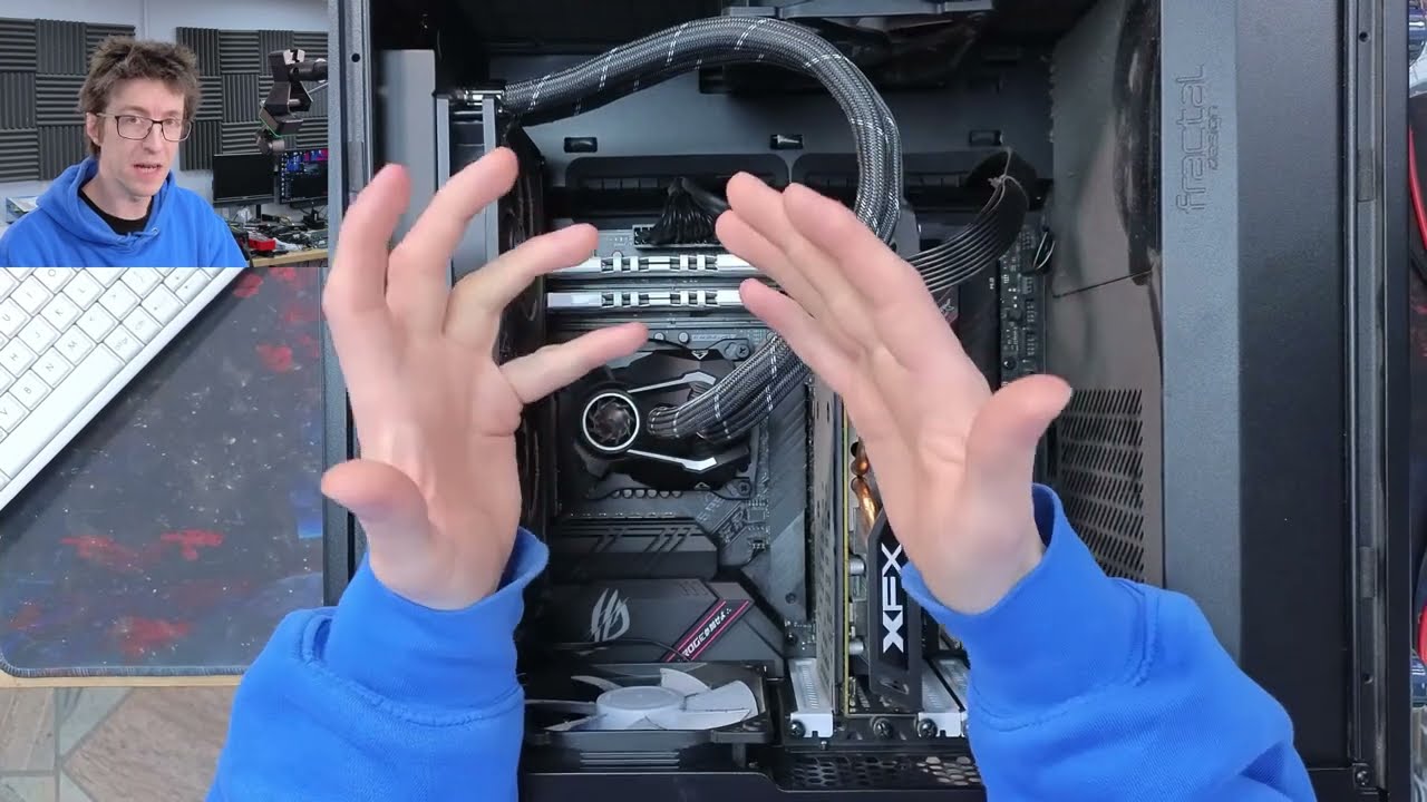
The dual chip setup that we're going to have a look today is a single BIOS chip that is spanned over two differently sized chips. So, let's roll the intro and get into it. This one feels to me like the BIOS has scrambled itself. Maybe it tried to install an update while it didn't have enough power. I don't know. But I think the BIOS on this is scrambled. So, I'm going to try and h and reflash the BIOS. So, uh let's take a let let me take you along for the ride on this one and I'll show you my methodology.
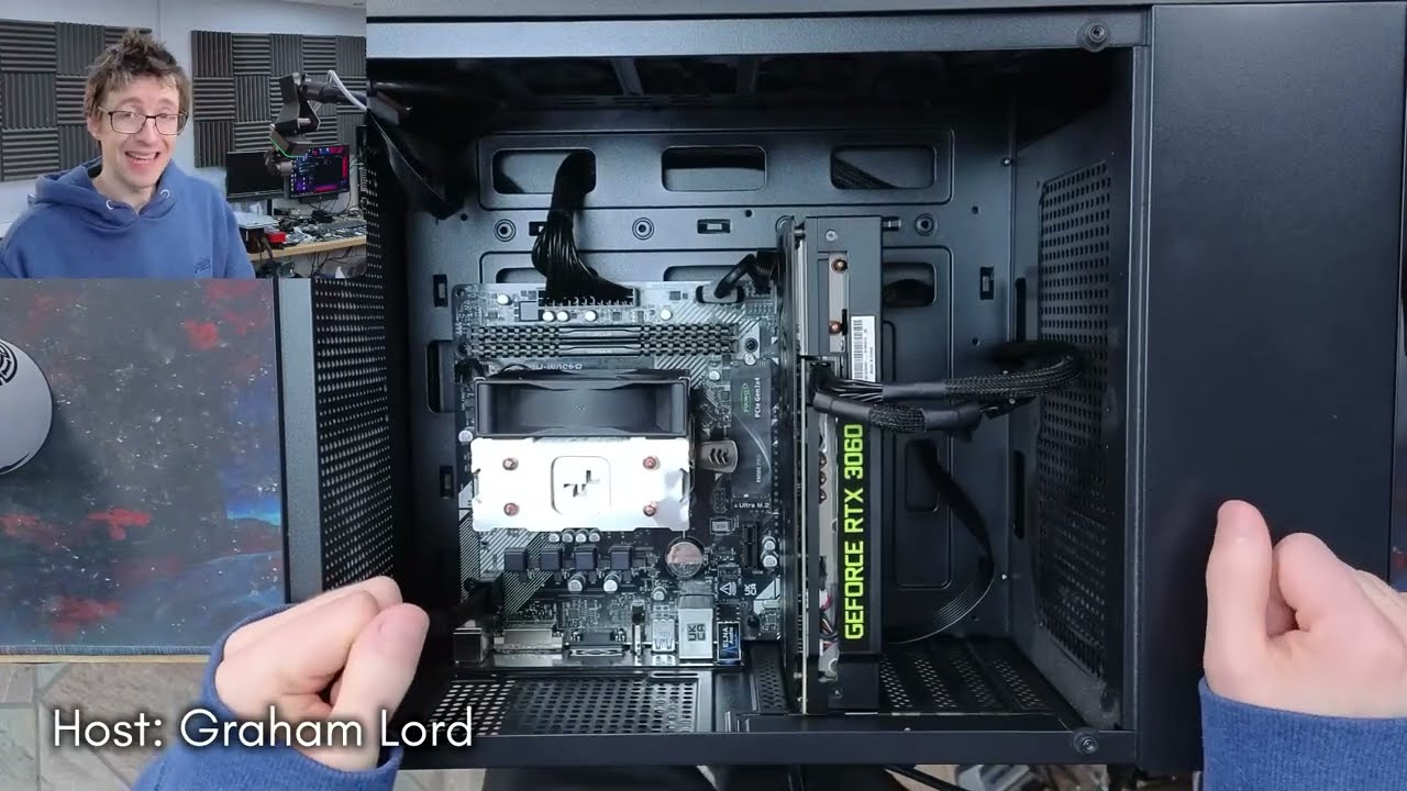
Now, this one's kind of an interesting example because it has two BIOS chips right next to each other that are different brands and different chip numbers, and I don't actually know which one has got the actual BIOS on it. Uh, and and which one is just something else, or uh it might be a dual chip BIOS configuration, which is strange to me on such a modern laptop, but you never know. So, this one's going to be a really good example of some of a slight curveball. Uh I'm going to start by taking the motherboard out from here just to get everything out the way because also I want to find out the board number.
Um and I'll tell you about that in a moment. So firstly, let's take this thing apart and get the motherboard out of it. So looking on the back of the motherboard here, if I peel back this foil that's just protecting the back, we've got some numbers down here. Um so one of these is the board number. I think it's NMD471. That's that looks like the most compelling to me. But we'll just make a mental note of all of these because we're going to need we might need to search for information on this later on. So just a mental note that that is there.
And on top we've got our two BIOS chips there and there. I've just removed the BIOS battery just to get it out of the way. Let's take a look under the microscope. So there's our two chips and those are So we've got a QMC that's a QH128 AHIG and then we've got a Wimbond 25 R64 JVSIQ. Now I did say in a previous video that um the chips are generally going to start with like 25. So that's 25 series SPI ROM. These QMC chips are weird, man. Um, they have slightly oddball names. Um, this is an SPI ROM and like the fact that it's got, you know, something something 128, you know, that's 128 megabits.
That's how I know that that's probably something. Um, and again, the positioning of it, uh, it's, uh, it's all on data lines. It's not next to power. Uh and also if we look at the marking here, we've got UB1, uh UB2, whatever that is, and then UB3. So again, the designators mean that these are all related things, you know. Um so, um like the B I'm guessing means BIOS. Um so, you know, these are indicators. These are signs, stuff that we can look out for. Now, the question is which one actually has the laptop BIOS on?
Well, I don't know. So, I'm going to check both of them. Now, if we looked up that board number and started doing some research, it might be that we could find someone online who's already figured this out. However, I'm a big believer in teaching people how to figure it out themselves. Um, because the issue is is like people often say like sort of, oh, why didn't you research it first? I'm like, yeah, you can do that, but you know what's more powerful is being the person who does the research. So, we can just look at the contents of both chips for ourselves.
So, let's do that. Um, now these are these chips are both in very annoying positions. They're right next to plastic stuff, which will melt easily under hot air. So, I'm actually going to try and go for my pogo pin strat here. Um, and I haven't done a lot of work with the pogo pins, but um, I'm going to give them a try at the very least just for reading the chips to see which one I need. um I can do a very quick read off of these and just find out what I'm dealing with. So firstly, let's just check what voltage these chips are.
So what was that again? That was a 25R64 JV. Let's look that up. And that's a 3V 64 megabit chip. So first of all, it being 64 megabit, that's kind of small. Um but again, we might have a dual BIOS system here. So uh so yeah, we'll come we'll we'll keep that in mind. but it's 3 volts. So, the other one is going to be 3 volts as well. But just to be careful, I'm going to check both. Right, this isn't a data sheet, but this is the QMC website, and they have confirmed there that it's a 25 QH1 128 uh 128 megabit.
So, that lines up. And again, it is a 3 3.3 volt chip. Well, 2.3 to 3.6. They have a range that they're comfortable with. Let's take a moment to talk through this dual chip setup that we're looking at and why it exists. In the video that I'm recording, I'm not yet certain if I'm looking at a dual chip configuration, but if we talk through it first, you can better understand it as I discover it in the video. So, what we're about to find is that the BIOS image is split across two different chips, a 16 megabyte chip and an 8 mgabyte chip.
That's 128 megabits and 64 megabits respectively. Remember in the last video when we opened up the ASUS capsule file in UEFI tool and there were multiple regions in the BIOS image. In a configuration like this, the main BIOS region will be on the larger chip and the smaller regions like the descriptor region and the ME region and things like that will be on the other chip on the smaller one. We're going to need the contents of both chips combined to make any sense of them. I'm going to talk about these different regions in the next video.
And so, for the time being, we don't really need to understand them. All that matters is that we have all of the regions in order to create the whole image. So, why would you do this at all? Why not just use a single bigger chip? Well, a larger chip might not have been available or cost effective at the time when the board was designed. There's going to be a price curve in price to capacity on the chip where the top capacity chip might end up being more than twice the price of the next one down.
So it would be cheaper to buy two smaller chips than one big chip. And also if your firmware image is say 12 MGB, well, it might be cheaper to buy an 8 MGAB chip and a 4 MGAB chip and use a dual chip configuration than a single 16 megabyte chip which can fit your entire image, but you're wasting a quarter of the chip that you paid a premium for. But also, this laptop is fairly modern, and 256 megabit or 16 megabyte chips aren't that exotic these days. But the CPU it has is one of those absolute potato Intel N series things.
And so it wouldn't surprise me in the least if someone said to me that the chip just simply doesn't support a 256 megabit BIOS chip. And so in which case, yeah, you'd have to use a 128 and a 64meg one combined for a 24 mgby BIOS image. So that's the brief. Let's dump the contents of these two chips and see what we find on them. Right, I'm going to try freehanding this because I just want the read right now. So, I'm going to press down there. I'm going to turn off pin detect because it's not going to work with the pogo pins.
And we're going to try and auto detect the chip. Nice. It recognizes it. 128a sic8. Close enough. Select and read. It worked on the pin detect anyway. Not bad. Okay, there we go. Right, we can go back. So, now we have some data. So, what I want to know now is, is this a complete BIOS image? Is this the thing we're looking for? So, firstly, we're going to save it. I got a tip off from the comments section in some of the previous videos that if I select flash here, that will trim out the meta data that the XG Pro software adds in.
So, that's nice to know. Thanks, folks. And with UEFI tool, I'm going to try and open that dump that I just took and we'll see what's inside it. Open. We've got an unaligned volume error on the parser and I'm not seeing this is an Intel system and I'm not seeing an ME region unless I'm blind. Um, so I'm going to grab the contents of the other chip as well and we'll just double check what's in that one. Cool. And we'll save that one out as well. Right. And that gives us an error. So there's not any kind of image here.
So this is either a a this is either another region, possibly our missing me region, um or it's not the BIOS, it's something else being stored on a ROM chip. So let's try and put these files together. Now, there are quick and easy ways that you can combine binary files using like Windows commands and stuff like that. But just for simplicity, I'm going to show you just doing this in a hex editor. So, uh I'm going to open Hexedit. So, I'm opening uh HXD here, which is a Windows hex editor. And we're just going to open both of these files in there.
So, let's just drag those in there. Um, and now when I opened the QMC chip, this had a this had a BIOS region in it, but it was missing an ME region and such, which may which leads me to believe that this is the main BIOS region, but the smaller chip, the Wind Bond one, this has all the other stuff in it, which means this one should go first. So, what I'm going to do is I'm going to scroll all the way to the bottom of this file. Uh, and I'm just going to put my cursor on the end of it there.
So, we're we've selected the bottom. Now, I'm going to go into here and I'm going to do control arr c. And I'm just going to paste that onto the end. And this is going to say this is going to change the file size. Yeah, I know I'm doing that. So, I've just pasted the contents of the QMC chip onto the end of the first one. And we're going to save this as a different file. Now let's save this as um combined.bin. So now when I have a look in here, I've now got this combined file that is a total of 24 megabytes, which is 16 + 8.
So let's uh let's load up uh UEFI tool again and let's try and look at that new combination file that we've made. So let's go into BIOS and combined. There we go. Now, that's what it's supposed to look like. We've got an Intel image. We've got a descriptor region. Um, uh, so there's all of our compatible chips and so on and so forth. We've got an ME region. There's our ME region. And then we've got the BIOS region. This was the contents of the QMC chip that we already had. So, as you can see, that looks the same.
So, we have a dual chip BIOS here. And we've just dumped both chips and then combined the contents into a single file. So, now we're getting somewhere. So, what we need to do now is we need to find a new BIOS for this. So, I'm going to do a quick bit of searching and see what I can find. I'm going to start by seeing if I can just get one directly from Lenovo. So, let's try our luck there. So, if I go over to the Lenovo website here, I've just pulled up the uh IdeaPad 317 ITL6 support page, drives and software, and under BIOS, we've got a BIOS update here.
So, this is 9.23 23 megabytes. That's not big enough to be a complete BIOS, but let's see what we get because it's probably compressed. So, I download that and it gives me this .exe file. Um, now an installer or an .exe file isn't a lot of use to us, but sometimes, and as is the case with this one, if you actually launch that into setup and just go through it a little ways, we'll see here, we have the option to extract only. So, let's do that. So, I'll just extract that into um uh Sure. Let's just use that default directory it selected.
Now, I'm just going to open that uh folder it gave me. And it gave me another .exe. Okay. If I open that, it's probably going to fail. This platform does not support this interface. Okay. Right. So, what I'm going to do now is I'm going to open task manager and I'm going to right click on that installer and do open file location. And that's opened up the temporary files where that installer has extracted to. So now we can see the payload of all the stuff it was going to install. And hey, look at that. There's a 26 megbyte file there.
That's exactly the correct size of our combined BIOS chips. M. So let's dump that in there. Copy that to there. Right now, we can close that. Let's tidy up because I'm starting to get buried under all of this nonsense. Oh, I lied. 26.579. It's slightly too big. Okay, let's have a look at this and see what it is. So, we'll pull up UFI tool and let's open that. Ah, it's a capsule file. Well, we've already looked at capsule files. We know how to deal with this. Now, if you're using a higherend programmer like a XGU Pro, um then the software for that would automatically know how to deal with a capsule file.
However, also we're not flashing an entire chip directly. So, that's still not going to work. So, we need to extract this. So, what I'm going to do is I'm going to right click on the Intel image and extract as is. So, let's put that in Intel.BIN. Right now, we're down to our raw BIOS. Now, we are at 24.576, which is correct. Now, we've got the correct file size. Now, we need to split this into our two separate chips. So, let's open it up in HXD. So, I'm going to drag that into HXD. Let's close the combined image.
And I'm also going to reopen our original Wimbond chip as well. So, so here's our new BIOS and we need to split this into two files and we need to know where to split it. So, if we look back at the Wimbond chip here, this was the smaller one. And if we scroll all the way down to the end of it, we can see that the final address is 007 FF FF0 007 FF FF0. So on the Intel chip, I'm going to scroll down to 07. If I was smart, I'd be using like a goto command or something like that.
But contrary to what these videos make me look, I'm not that smart. I've just figured out how to get through this. There we go. 007 FF FF0. So, we want to grab everything from this point downwards. So, I'm going to place my pointer at 8. Scroll to the bottom. And I'm going to hold down shift and click. So now we've grabbed everything uh now we've grabbed everything from block 08 onwards to the end of the file. And I'm going to Ctrl X. Yes, this will change the file size. And then we're going to make a new file and Ctrl +V.
All right. So now this one we're going to save as. This is our small one. So, we're going to call this windbond new.bin. And this is our larger file. And we'll save this as QMC new.bin. And now we've just extracted our two chip image files. And as you can see, one of them is 8 megabytes and the other is 16 megabytes on the dot. Remember, the file sizes must be on the dot. So, we have something that's ready to go now. Um, however, I would like to be able to preserve the serial number and product data uh and product key uh number on this laptop.
And I've just spent a bunch of time digging through the BIOS trying to find this data so I can transfer it over and I couldn't find it. Um, so, um, however, also I have seen that there are utilities online to update the serial number on the laptop after the fact. So, I'm going to start flashing the BIOS and we'll solve we'll cross that bridge when we get to it. The one thing to bear in mind is that the Windbon chip has the ME region on it. Uh, and the XMC has all of the user data, has the rest of the BIOS, but also the um unique data such as serial number and so on on it.
So, I'm going to start by just flashing the windbond chip. This will update the ME region to a cleaned me region. So, let's try that and see if that does the job. And if that doesn't do it, I'll try flashing the other chip as well. And that will that should at least get us a laptop that turns on and starts, even if we have to do extra work with it afterwards. So, let's try that. Um, sometimes when in doubt, uh, even if you're missing a bunch of serial data that you need, um, you will at least get a computer that turns on and posts.
So, if you get that far, you know that messing with the BIOS is going to actually get you there. So, a lot of the time I will flash just a clean BIOS with no serial data on it onto a laptop because if it then turns on, then I know it's worth actually spending the time messing around with the serial data. Otherwise, I could spend half an hour messing around with this BIOS and I don't even know if this is going to fix the laptop yet. So, let's just flash something on there and see if it works.
So, going back to XG Pro, I'm going to load up my new uh Wimond file. So, wind bond new. Let's open that. And I've already got the Wind Bond chip selected because that was the one that I did second. Let's go ahead and flash that. And let's go ahead and program. Programming finished. credit where it's due. These pogo pin things pretty good. If you didn't have a high-speed programmer, I wouldn't be having fun with this thing. But if you've got a high-speed programmer like a like an XG Pro, yeah, this is pretty decent. Not going to lie, I'm into it.
I might go so far as to say that I am a true believer in the pogo pins. Now, No, it has exactly the same problem as it had before. So, I don't think this is a BIOS issue. I think there's something else wrong with it. So, once again, I leave you on a repair that didn't actually work, which was not deliberate. However, it was a really good example of showing you how to approach these dual chip systems and how you can break down BIOS images and put them back together again. That's the bit that I wanted to teach in this video.
So, um, in it's also a good lesson that sometimes you will do this and it's not just going to magically fix your laptop. Sometimes clean me bro just doesn't work, which is effectively what happened here. But I hope you guys found it interesting to see how we can break down and rebuild those BIOS images. So in the next video, I want to start getting deeper into the BIOS image itself and start talking about the regions within the BIOS image, what they do, and how we can start manipulating data inside them. So, thank you very much for watching.
I hope you guys found that interesting, and I'll see you soon. Bye for now.
More from Adamant IT
Get daily recaps from
Adamant IT
AI-powered summaries delivered to your inbox. Save hours every week while staying fully informed.